23 Bach Dang Street, Tan Son Hoa Ward, Ho Chi Minh City, Vietnam
mr.phamgiakhang@gmail.com


Exploring EDS & CL Technology for Semiconductor and Lithium-ion Battery Material Analysis
In semiconductor research, advanced materials, and next-generation batteries, surface morphology alone is not enough. It is equally important to understand which elements are present, where they are distributed, and how material properties change at the microscopic level.
At a technical seminar held at Ho Chi Minh City University of Technology and Education (HCMUTE), advanced material analysis solutions within the Gatan – EDAX ecosystem of AMETEK were introduced. One of the highlights was the ability to correlate EDS (Energy Dispersive X-ray Spectroscopy) and CL (Cathodoluminescence) data from the same region of a sample.
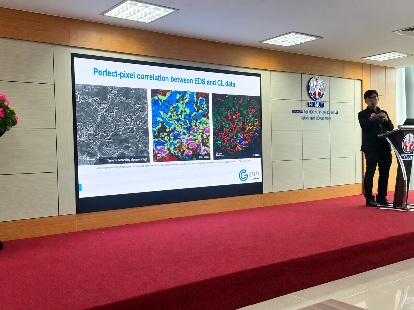
Figure 1. Demonstration of pixel-level correlation between EDS and CL data for advanced material analysis.
EDS – Energy Dispersive X-ray Spectroscopy is an elemental analysis technique commonly integrated with SEM and TEM systems.
When an electron beam interacts with a sample, characteristic X-rays are generated. By detecting these X-rays, EDS can help identify:
Elemental Mapping visualizes the distribution of elements using color-coded maps, helping researchers understand the relationship between microstructure and chemical composition.
EDS is widely applied in semiconductor, electronics, battery, advanced materials, metallurgy, and failure analysis applications.
One of the key technologies presented during the seminar was the capability for “perfect-pixel correlation between EDS and CL data.”
While EDS helps answer:
“Which elements are present at this location?”
Cathodoluminescence (CL) provides additional information about the optical emission of a material when stimulated by an electron beam.
By combining these techniques on the same analytical region, researchers can correlate:
Microstructure → Elemental Composition → Optical Properties
This approach is particularly valuable for applications such as:
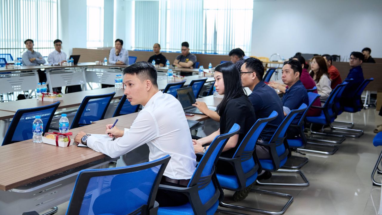
Figure 2. Technical discussion on advanced electron microscopy and material characterization technologies.
Another important application of EDS is the characterization of Lithium-ion battery materials.
A Lithium-ion battery contains multiple layers and different material systems. Even relatively small variations in elemental composition, contamination, or material distribution may influence cell performance, stability, and lifetime.
SEM combined with EDS can be used to investigate:
Cathode – Anode – Separator – Particles – Coatings – Battery cross-sections
For example, in NMC – Nickel Manganese Cobalt cathode materials, EDS can generate elemental maps for elements such as:
Ni – Mn – Co – O
This enables researchers to evaluate material uniformity, differences between particles, and regions with abnormal composition.
EDS is also highly useful for Failure Analysis, especially when identifying contamination or unexpected elements associated with a failure location.
One important challenge in battery characterization is that Lithium is difficult to detect directly using conventional EDS.
Lithium has a very low atomic number and produces extremely low-energy characteristic X-rays. As a result, traditional EDS techniques have significant limitations when attempting to directly detect and quantify Lithium.
This is where complementary analytical approaches become important.
One notable solution from Gatan is the Cipher System, which combines:
EDS + quantitative Backscattered Electron Imaging (qBSE) + DigitalMicrograph
to support Lithium distribution analysis using the Lithium by Composition by Difference (Li-CDM) methodology.
Rather than relying solely on the weak X-ray signal generated by Lithium, this approach combines compositional information from EDS with quantitative backscattered electron data to determine Lithium distribution within the material.
This methodology can support the investigation of battery materials such as:
Modern electron microscopy is no longer limited to simply providing high-magnification images.
By integrating techniques such as:
EDS – CL – EELS – BSE – EBSD
researchers can obtain a more comprehensive understanding of materials, including:
Structure + Chemical Composition + Elemental Distribution + Functional Properties
These capabilities are particularly valuable in industries requiring high-precision characterization, including semiconductor manufacturing, advanced packaging, battery technology, electronics, and material research.
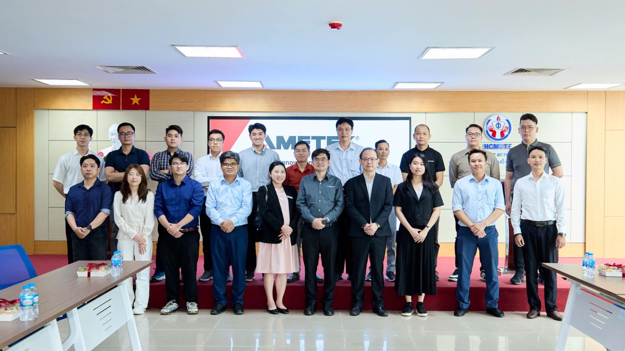
Figure 3. Participants at the technical seminar and material characterization discussion at HCMUTE.
The seminar provided an opportunity to explore advanced material characterization technologies and gain a deeper understanding of how multiple analytical techniques can be integrated with electron microscopy.
In particular, the correlation of EDS and CL data, together with advanced approaches for Lithium-ion battery material analysis, offers powerful tools for research, quality control, and failure analysis.
VietnamSemi will continue to share new technologies, equipment, and applications in semiconductor, electronics, advanced materials, and energy storage.
